Electronic and semiconductor
Laser technology has been used in the electronics for a few years now and it has helped many consumer electronics companies to provide better products for their customers.
Laser marking, laser cutting is the most common technology used on electronics.
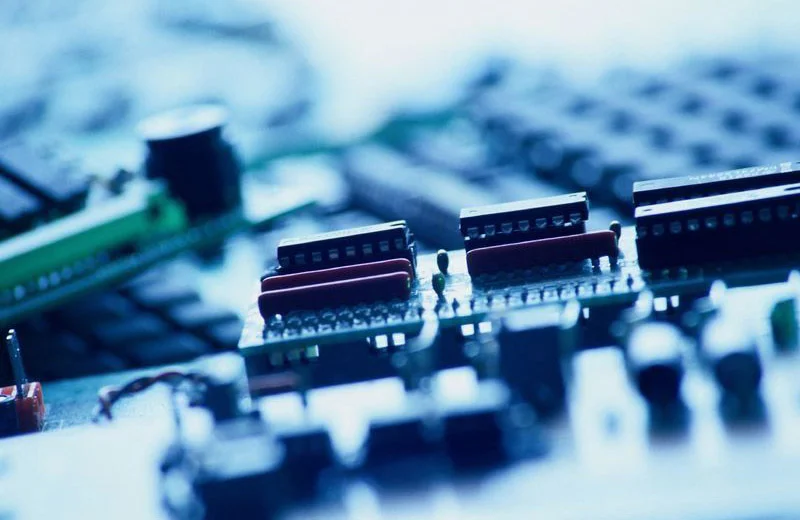
High quality requirements and absolutely complete information flow in every process step are the requirements in the field of electronics. Circuit boards and electronic components are marked with permanent, solder-resistant and safe machine-readable laser markings, for example a data matrix code. The laser system can read the information to be inscribed directly from a database, mark it on the component and check it for quality and content through a camera system. With the use of a camera system, the position and orientation can be detected, the caption can be automatically adjusted, and the content and quality can be checked. Thus you achieve high quality assurance as well as high production efficiency. Fully automated laser systems with automatic loading and unloading of printed circuit boards, for example, guarantee high efficiency and high volume flow.
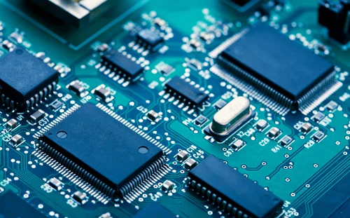
Semiconductors and small electronic components are usually produced in very large quantities. Economic mass production is only possible through fully automated processes. The small components often have to be provided with much information. This information must be flexibly and extremely quickly applied to the components. By using a laser system with a galvo head for very fast deflection of the laser beam and a partially or fully automated solution, the high requirements can be met. The applied marking is resistant, durable and perfectly readable. A laser system is also used for special test procedures of microchip testing, also called decapping. Decapping a microchip into a process of removing the protective coating of a microchip so that the actual chip itself is revealed for visual inspection of the microcircuits. This process is typically performed to debug a manufacturing problem with the chip or possibly copy information from the chip.
