


Fast! Accurate! Steady! Han's laser creates a powerful brand for semiconductor wafer detecting
According to SEMI statistics, the market scale of global semiconductor equipment in 2020 is US $59.8 billion, a year-on-year increase of 19%, reaching a record
high of US $71.2 billion. China became the world's leading semiconductor equipment market for the first time. In 2020, the market scale increased by 39% to US
$18.72 billion.
There is a huge market space for semiconductor wafer detecting equipment
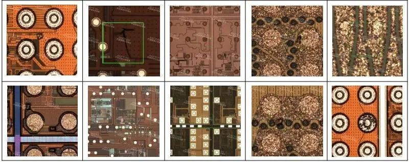
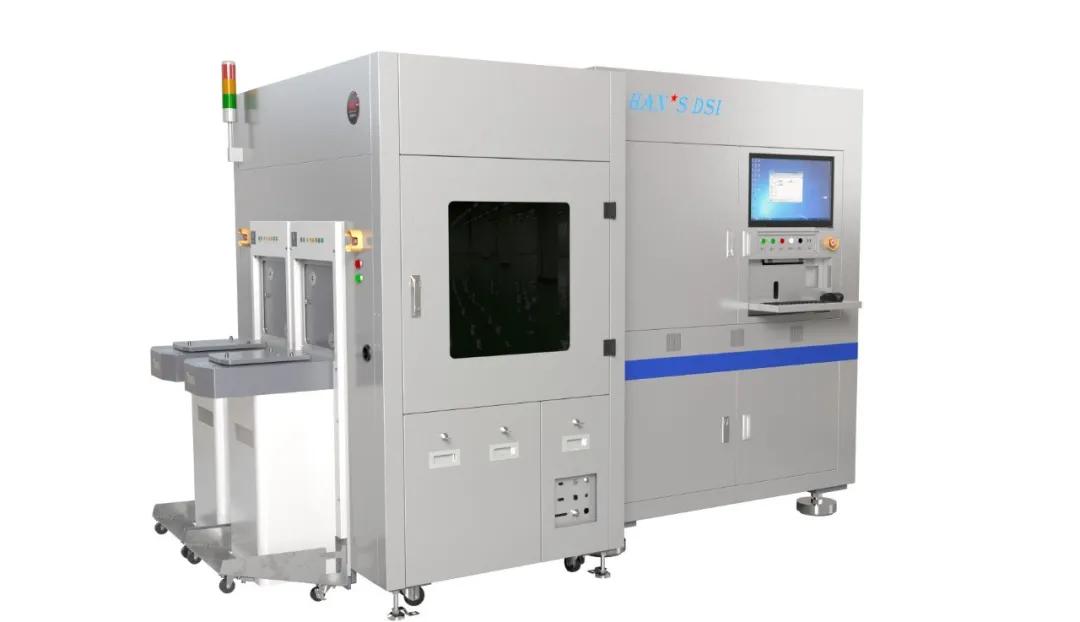
Han’s laser has launched the latest series of detecting products: IFOX series automatic optical wafer detecting equipment. The equipment is suitable for 2D macro
defect detection, dimension measurement and 3D bump measurement of 8-12 inch bare wafers and frame wafers, and can realize multi-dimensional detection of
various characteristics of wafers.
IFOX series automatic optical wafer detecting equipment
Advantages of equipment
1. Fast:
● Imaging quality: use the most advanced camera technology to achieve ultra fast scanning with minimal aberration;
● Measurement integration package: Han's laser is the first company to use measurement integration package, which can create a fast measurement scheme in a simple and convenient way;
2. Accurate:
● Optical system: the use of independent and advanced large field microscope, equipped with advanced lighting system and real-time focusing technology;
● Defect search: use advanced intelligent defect algorithm to overcome the variation caused by process technology;
● Linear high precision motor, XYZ platform, 100 nm resolution;
● Mechanical structure, 200 nm precision;
3. Steady:
● Clean and clean design (the moving platform is on the underside of the wafer);
● Floating base platform reduces the impact of equipment vibration.
high of US $71.2 billion. China became the world's leading semiconductor equipment market for the first time. In 2020, the market scale increased by 39% to US
$18.72 billion.
There is a huge market space for semiconductor wafer detecting equipment
Han’s laser has launched the latest series of detecting products: IFOX series automatic optical wafer detecting equipment. The equipment is suitable for 2D macro
defect detection, dimension measurement and 3D bump measurement of 8-12 inch bare wafers and frame wafers, and can realize multi-dimensional detection of
various characteristics of wafers.
IFOX series automatic optical wafer detecting equipment
Advantages of equipment
1. Fast:
● Imaging quality: use the most advanced camera technology to achieve ultra fast scanning with minimal aberration;
● Measurement integration package: Han's laser is the first company to use measurement integration package, which can create a fast measurement scheme in a simple and convenient way;
2. Accurate:
● Optical system: the use of independent and advanced large field microscope, equipped with advanced lighting system and real-time focusing technology;
● Defect search: use advanced intelligent defect algorithm to overcome the variation caused by process technology;
● Linear high precision motor, XYZ platform, 100 nm resolution;
● Mechanical structure, 200 nm precision;
3. Steady:
● Clean and clean design (the moving platform is on the underside of the wafer);
● Floating base platform reduces the impact of equipment vibration.